Understanding Bias Circuits for RF Power Amplifiers
RF power amplifiers (PAs) are essential in many applications, from amateur radio and wireless communications to radar systems and broadcasting. One of the most critical aspects of designing or building an RF PA is the bias circuit for RF power amplifiers. A properly designed bias circuit ensures stable operation, good linearity, high efficiency, and protection against thermal runaway—especially important with modern high-power transistors like LDMOS or GaN devices.
In this post, we'll explore why bias circuits matter, the common types used in RF PAs, and some practical considerations for getting them right.
Why Biasing Matters in RF Power Amplifiers
The bias circuit sets the quiescent (no-signal) operating point of the transistor. In RF PAs, this directly affects:
- Linearity – Critical for avoiding distortion in modulated signals.
- Efficiency – Classes like AB or C need precise bias for optimal power added efficiency (PAE).
- Stability – Prevents thermal runaway, where heat causes increased current, leading to device failure.
- Reliability – Especially under varying temperature or VSWR conditions.
A poor bias design can turn an otherwise excellent amplifier into an unreliable or inefficient one.

A typical sequential bias circuit example, ensuring gate bias is applied before drain voltage in pulsed applications.
Common Types of Bias Circuits for RF Power Amplifiers
- Fixed Bias
Simple resistor divider or voltage source to set gate/base voltage. Easy to implement but sensitive to temperature changes and device variations. - Self-Bias
Uses a source/emitter resistor with bypass capacitor. Provides some negative feedback for stability but reduces gain. - Active Bias
Uses transistors, op-amps, or dedicated ICs to regulate bias current/voltage. Offers excellent temperature compensation and stability. Very common in modern high-power RF designs. - Sequenced Bias
Ensures gate bias is established before applying drain/collector voltage, protecting the transistor during power-up—critical for GaN and LDMOS devices.

An example of a more complex bias sequencing and active regulation circuit.
Practical Examples and Real-World Implementations
In practice, many builders start with kits or commercial modules that include well-engineered bias circuitry. These save time and reduce the risk of instability.

A high-power LDMOS amplifier board showing integrated bias networks and matching components.
Professional modules often incorporate temperature-compensated active bias regulators and protection features.
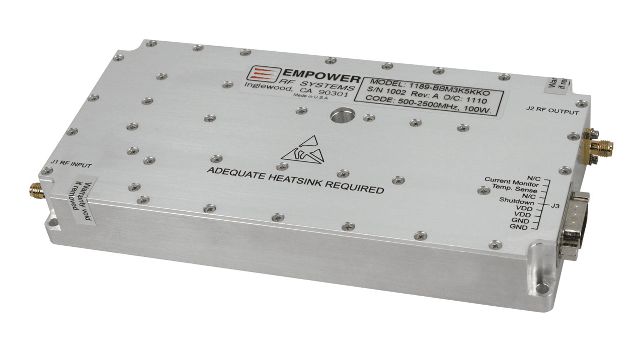
A commercial-grade solid-state RF power amplifier module with robust design.
When selecting components or ready-made solutions, manufacturers like ZR Hi-Tech stand out for their reliable RF power amplifier modules that feature carefully optimized bias circuits, delivering consistent performance across a wide range of frequencies and power levels.
Final Thoughts
Getting the bias circuit for RF power amplifiers right is half the battle in achieving a stable, efficient, and long-lasting design. Whether you're building from scratch or using pre-built modules, understanding these principles will help you make better choices.
If you're working on an RF project, consider exploring high-quality options from established RF power amplifier manufacturers—ZR, for example, offers excellent solutions tailored for demanding applications.
Have you built your own RF PA? Share your bias circuit experiences in the comments!


Comments
Post a Comment